Optical transistor based on a photonic crystal with Raman defect
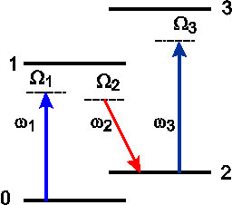
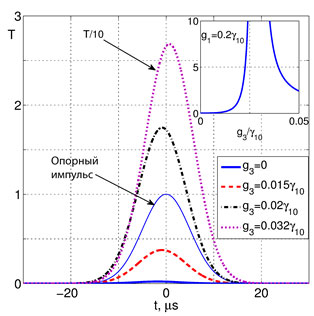
We proposed a new type of all-optical switch based on 1D photonic crystal (PC) with the defect doped with a four-level N-type active Raman gain medium (Fig. 5_1a). Transmission and reflection of a probe (Raman) beam strongly depend on the switching field intensity and can be greatly amplified or attenuated. Therefore, the optical switching field can serve as a transistor gate field to effectively control propagation of a weak probe field. The group velocity of the probe pulse can be controlled in the range from subluminal (slow light) to superluminal by varying the pump field intensity (fast light) (Fig.5_1b).
 |
 |
| Fig. 5_1. (a) Energy diagram of the active Raman medium interacting with three fields: weak probe (Raman) field of frequency ω2 and controlling and switching fields with frequencies ω1 and ω3, respectively. | Fig. 5_1. (b) Time dependence of the probe pulse transmitted through a PC cavity with ARG medium for different switching Rabi frequencies at the entrance into the PC g3. The thin solid curve illustrates a reference pulse (empty PC cavity and g3 = 0). The incident Gaussian probe pulse length is 20 μs. Right inset: probe field transmittance vs g3. |
- V. G. Arkhipkin, S. A. Myslivets. All-optical transistor using a photonic-crystal cavity with an active Raman gain medium // Phys. Rev. A, 2013. V.88, 0333847-1 - 0333847-6.
